G12 Monocrystalline Silicon Wafer Market Projected at $16.38 Billion by 2025: Key Momentum in China, South Korea, and Germany
The G12 Monocrystalline Silicon Wafer Market is projected to reach $16.38 billion by 2025, driven by rising demand for efficient solar energy solutions and advancements in photovoltaic technology. Key growth factors include China’s manufacturing leadership, geopolitical influences on the supply chain, and innovations in wafer production. This market overview highlights emerging trends, challenges, and regional dynamics shaping the future of G12 wafers in renewable energy applications.
- Last Updated:
G12 Monocrystalline Silicon Wafer Market: Q1 and Q2 of 2025 Analysis
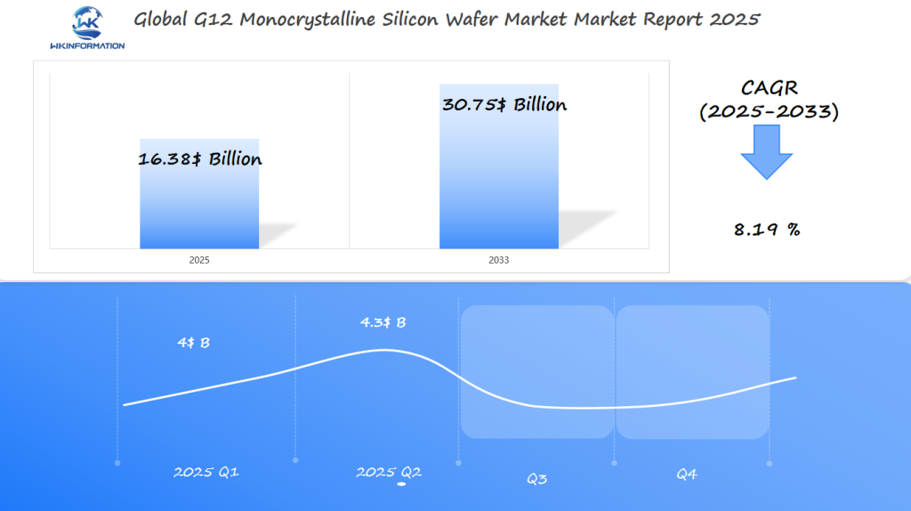
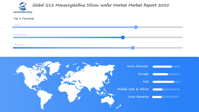
The G12 Monocrystalline Silicon Wafer market is expected to reach $16.38 billion by 2025, with a CAGR of 8.19% during the 2025–2033 period. In Q1 2025, the market is projected at $4 billion, with growth continuing through Q2 to $4.3 billion. These wafers are a key component in the production of high-efficiency solar cells, and their demand is rising as the world transitions to renewable energy sources. China, South Korea, and Germany are the largest consumers of G12 wafers, with China being the dominant player in manufacturing and export. South Korea is heavily investing in solar energy production, making wafers critical to its solar panel industry. Germany, with its strong focus on sustainability and renewable energy infrastructure, is also contributing to the growing demand. The rise in global solar power installations, coupled with innovations in wafer technologies, will drive the market forward in the coming years.
Key Takeaways
- The G12 Monocrystalline Silicon Wafer Market is projected to reach $16.38 Billion by 2025.
- China is a key driver of this growth due to its increasing adoption of renewable energy.
- Advancements in photovoltaic technology are enhancing the efficiency of solar panels.
- The silicon wafer industry is crucial for the development of more efficient solar panels.
- The market’s expansion is fueled by the need for durable and efficient solar wafers.
Overview of the Upstream and Downstream Industry Chain in the G12 Monocrystalline Silicon Wafer Market
The G12 Monocrystalline Silicon Wafer market operates within a complex ecosystem that involves both upstream and downstream industry chains. This intricate relationship between different segments of the industry is crucial for understanding the market’s dynamics.
Understanding the Industry Chain
The G12 Monocrystalline Silicon Wafer industry chain consists of several key components. Upstream, the production of high-purity silicon is critical. This raw material is then processed into wafers, which are used downstream in the manufacturing of solar cells and modules.
Upstream Segment
The upstream segment involves the production of high-purity silicon, a process that requires significant technological expertise and investment in equipment. High-purity silicon production is the foundation of the G12 Monocrystalline Silicon Wafer industry.
Downstream Segment
Downstream, the wafers are used in the production of solar cells and modules. This segment is driven by demand from the solar energy sector, which is increasingly adopting G12 Monocrystalline Silicon Wafers due to their efficiency and cost-effectiveness.
| Industry Chain Segment | Key Activities | Key Players |
| Upstream | Production of high-purity silicon | Silicon manufacturers |
| Midstream | Wafer production | Wafer manufacturers |
| Downstream | Solar cells and modules production | Solar panel manufacturers |
Trends Influencing the G12 Monocrystalline Silicon Wafer Sector
The G12 Monocrystalline Silicon Wafer industry is undergoing a significant change driven by technological advancements and market demands. This change is marked by:
- The increasing adoption of larger wafer sizes
- Improvements in manufacturing processes
- A growing focus on sustainability
Emerging Trends
Several emerging trends are crucial in shaping the G12 Monocrystalline Silicon Wafer sector. These include the shift towards larger wafer sizes to enhance efficiency and reduce costs, and advancements in technology that improve the quality and performance of wafers.
Technological Advancements
Technological innovations are essential in the G12 Monocrystalline Silicon Wafer industry. Key advancements include:
- Improved manufacturing processes that reduce defects and increase yield.
- Enhanced material quality leading to better performance of solar cells.
- Innovations in wafer cutting and handling that minimize damage and improve efficiency.
The integration of these technological advancements is expected to drive the G12 Monocrystalline Silicon Wafer market forward, enabling the production of more efficient solar cells at lower costs. As the industry continues to evolve, staying updated with these trends will be crucial for stakeholders.
Constraints impacting G12 Monocrystalline Silicon Wafer development
The development of G12 Monocrystalline Silicon Wafers is not without its hurdles, including high production costs and manufacturing complexities.
One of the significant challenges in G12 Monocrystalline Silicon Wafer development is the high cost associated with producing these wafers. The manufacturing process involves complex technologies and high-purity materials, contributing to the elevated costs.
Challenges in Development
The silicon wafer industry faces constraints related to the production of large-sized wafers without defects. As wafer sizes increase, maintaining uniformity and reducing defects become more challenging.
To overcome these challenges, manufacturers are investing heavily in research and development to improve manufacturing technologies and reduce production costs. This includes advancements in crystal growth techniques and wafer processing.
The industry is also exploring new materials and technologies that can help mitigate some of the current constraints. For instance, advancements in wire sawing technology can help reduce kerf loss and improve wafer yield.
Furthermore, the industry is focusing on improving the efficiency of solar cells made from G12 Monocrystalline Silicon Wafers. This involves developing better cell architectures and manufacturing processes.

Geopolitical considerations in G12 Monocrystalline Silicon Wafer supply
Global trade policies and international relations have a significant impact on the supply of G12 Monocrystalline Silicon Wafers. The complex dynamics of global geopolitics can either make it easier or harder for the supply chain to operate smoothly.
The G12 Monocrystalline Silicon Wafer industry is highly sensitive to changes in geopolitical situations. Factors such as trade tariffs, export restrictions, and diplomatic relations between countries can greatly affect the availability and pricing of silicon wafers.
Global Trade Dynamics
The global silicon wafer supply chain is complex, involving multiple countries and companies. Geopolitical factors can disrupt this supply chain in various ways:
- Trade Tariffs: Imposition of tariffs on silicon wafers or related materials can increase costs and affect supply chain efficiency.
- Export Restrictions: Restrictions on the export of critical materials or technologies can limit the production capacity of certain manufacturers.
- Diplomatic Relations: Strained diplomatic relations between countries can lead to supply chain disruptions and impact the global availability of G12 Monocrystalline Silicon Wafers.
To navigate these challenges, companies involved in the G12 Monocrystalline Silicon Wafer market must stay informed about geopolitical developments and adapt their supply chain strategies accordingly.
Understanding the geopolitical landscape is crucial for companies to mitigate risks and capitalize on opportunities in the global G12 Monocrystalline Silicon Wafer market. By closely monitoring geopolitical factors, businesses can develop more resilient supply chains and maintain a competitive edge.
Segmenting G12 Monocrystalline Silicon Wafers by type
G12 Monocrystalline Silicon Wafers are categorized into different types based on their characteristics. This segmentation is vital for manufacturers and consumers alike, as it helps in tailoring production and selecting the appropriate wafers for specific applications.
The types of G12 Monocrystalline Silicon Wafers are primarily distinguished by their resistivity, thickness, and surface orientation. These characteristics play a crucial role in determining the wafer’s suitability for various applications, including solar energy and electronics.
Characteristics and Applications
The resistivity of G12 Monocrystalline Silicon Wafers is a critical factor, as it affects their efficiency in converting sunlight into electricity. Wafers with lower resistivity are generally preferred for high-efficiency solar cells.
Thickness is another important characteristic, with thinner wafers being more cost-effective and reducing material usage. However, they must be thick enough to maintain structural integrity during the manufacturing process.
The surface orientation of the wafer, typically categorized as (100), (110), or (111), influences its electronic properties and the efficiency of the solar cells produced.
| Type Resistivity (Ωcm) Thickness (μm) Surface Orientation Primary Application Type I | 1-10 | 180-200 | (100) | Solar Energy |
| Type II | 0.1-1 | 150-180 | (110) | Electronics |
| Type III | 10-100 | 200-250 | (111) | High-Efficiency Solar Cells |
Understanding these segments and their characteristics is essential for both manufacturers and consumers to make informed decisions. The diversity in types of G12 Monocrystalline Silicon Wafers caters to a wide range of applications, driving innovation and efficiency in the industry.
Exploring the diverse applications of G12 Monocrystalline Silicon Wafers
The versatility of G12 Monocrystalline Silicon Wafers is evident in their wide range of applications. These wafers are primarily used in the production of solar cells due to their high efficiency and ability to convert sunlight into electricity. For instance, the G12 Monocrystalline Silicon Wafers are a popular choice in the renewable energy sector.
The high performance of these wafers is attributed to their unique monocrystalline structure, which allows for better electron mobility and thus higher efficiency in energy conversion.
Applications in Solar Energy
G12 Monocrystalline Silicon Wafers play a crucial role in the solar energy sector. Their high efficiency makes them ideal for use in solar cells, contributing to the generation of clean energy. The growing demand for renewable energy sources is driving the demand for these wafers.
The use of G12 Monocrystalline Silicon Wafers in solar panels enables the production of high-efficiency solar cells. These solar cells are then used in various solar panel configurations to generate electricity. The efficiency and reliability of G12 Monocrystalline Silicon Wafers make them a preferred choice for solar energy applications.
Key Benefits of G12 Monocrystalline Silicon Wafers in Solar Energy
- High efficiency in converting sunlight into electricity
- Reliability and durability in various environmental conditions
- Contribution to the generation of clean and renewable energy
The demand for G12 Monocrystalline Silicon Wafers is expected to continue growing as the world shifts towards renewable energy sources. Their applications in solar energy are not only limited to solar cells but also extend to other areas such as concentrated photovoltaic (CPV) systems.
G12 Monocrystalline Silicon Wafer Market Growth in Different Regions
The G12 Monocrystalline Silicon Wafer market is growing at different rates in various parts of the world. This growth is influenced by factors such as government policies, the demand for solar energy, and the location of manufacturing facilities in each region.
Regional Market Analysis
Regional market analysis is crucial for understanding the G12 Monocrystalline Silicon Wafer market. Different regions exhibit unique trends and growth patterns due to varying factors.
North America
The North American market is driven by the increasing demand for solar energy and government incentives for renewable energy projects. The presence of key industry players also contributes to market growth.
Europe
Europe is witnessing significant growth in the G12 Monocrystalline Silicon Wafer market due to stringent environmental regulations and government support for solar energy.
Asia Pacific
The Asia Pacific region dominates the G12 Monocrystalline Silicon Wafer market, driven by the presence of major manufacturing hubs in countries like China and South Korea.
China’s Role as a Manufacturing Hub for G12 Monocrystalline Silicon Wafers
China’s dominance in the G12 Monocrystalline Silicon Wafer market can be attributed to its advanced manufacturing capabilities and favorable government policies. The country’s large-scale production facilities, coupled with significant investments in technology and infrastructure, have positioned it as a leading player in the global market.
China’s Manufacturing Capabilities
China’s manufacturing capabilities are a key factor in its success as a G12 Monocrystalline Silicon Wafer manufacturing hub. The country has modern production facilities that allow for the production of high-quality wafers at competitive prices. Advanced technologies and manufacturing methods have been implemented to ensure the production of wafers that meet the strict standards of the solar industry.
The government’s support for the solar industry has also played an important role in China’s rise as a manufacturing hub. Favorable policies and incentives have encouraged investment in the sector, leading to growth and development.
South Korea’s innovation in wafer technology
South Korea is leading the way in wafer technology innovation, making significant progress in the G12 Monocrystalline Silicon Wafer market. The country’s strong research and development infrastructure, along with major investments from top companies, is driving the industry forward.
According to industry experts, “South Korea’s commitment to advancing wafer technology is evident in its state-of-the-art manufacturing facilities and innovative production techniques.” These advancements are essential for improving the efficiency and lowering the production costs of G12 Monocrystalline Silicon Wafers.
Advancements in Wafer Technology
South Korean companies are leveraging cutting-edge technologies to enhance wafer quality and performance. Key areas of focus include improving crystal purity, reducing defects, and increasing wafer diameter. These advancements are critical for meeting the growing demand for high-efficiency solar cells and semiconductor devices.
The impact of these innovations is significant, with potential applications extending beyond the solar industry to electronics and other sectors. As one industry leader noted, “The future of wafer technology lies in its ability to adapt to emerging trends and technologies, and South Korea is well-positioned to lead this charge.”
G12 wafer technology advancements
- Enhanced crystal growth techniques
- Advanced wafer slicing methods
- Innovative surface treatment processes
These developments are not only improving the performance of G12 Monocrystalline Silicon Wafers but also contributing to the overall growth of the renewable energy and semiconductor industries.
Germany’s renewable energy demand fueling wafer growth
Germany’s strong commitment to renewable energy is significantly influencing the demand for G12 Monocrystalline Silicon Wafers. The country’s policies supporting solar energy adoption are creating a favorable environment for the growth of the wafer market.
Impact of Renewable Energy Demand
The increasing demand for renewable energy in Germany is directly impacting the G12 Monocrystalline Silicon Wafer market. The country’s Energiewende (Energy Transition) program is a key factor driving this demand, as it aims to reduce greenhouse gas emissions and increase the share of renewable energy in the energy mix.
The demand for G12 Monocrystalline Silicon Wafers is expected to rise as Germany continues to invest in solar energy. This investment is not only limited to new solar panel installations but also includes the upgrade and replacement of existing infrastructure, further boosting the demand for high-efficiency wafers.
What’s next for the G12 Monocrystalline Silicon Wafer market?
As the world shifts towards renewable energy sources, the future of the G12 Monocrystalline Silicon Wafer market looks increasingly promising.
The G12 Monocrystalline Silicon Wafer market is expected to witness significant growth driven by the increasing demand for solar energy and advancements in wafer technology.
Future Outlook
The future outlook for the G12 Monocrystalline Silicon Wafer market is characterized by several emerging trends. One of the key trends is the continued advancement in wafer technology, which is expected to improve efficiency and reduce production costs.
Another significant trend is the expansion of manufacturing capacities, particularly in regions with strong support for renewable energy.
Key Trends Shaping the Future:
- Increased adoption of bifacial solar panels
- Advancements in PERC technology
- Expansion of manufacturing capacities in Asia
The table below summarizes the key trends and their expected impact on the G12 Monocrystalline Silicon Wafer market.
| Trend | Expected Impact | Timeframe |
| Advancements in Wafer Technology | Improved Efficiency, Reduced Costs | 2025-2030 |
| Expansion of Manufacturing Capacities | Increased Supply, Lower Prices | 2023-2028 |
| Adoption of Bifacial Solar Panels | Increased Demand for High-Efficiency Wafers | 2024-2032 |
The future of the G12 Monocrystalline Silicon Wafer market is bright, with emerging trends and technological advancements expected to drive growth and innovation.
Competitive Landscape of the G12 Monocrystalline Silicon Wafer Market
The G12 Monocrystalline Silicon Wafer market is highly competitive, with major players such as LONGi Green Energy Technology Co., Ltd., JinkoSolar Holding Co., Ltd., and JA Solar Technology Co., Ltd. leading the industry. These companies are implementing different strategies to stay ahead in the market.
Key Players
- LONGi Green Energy Technology Co., Ltd. – China
- Tongwei Co., Ltd. – China
- JA Solar Technology Co., Ltd. – China
- Trina Solar Limited – China
- GCL-Poly Energy Holdings Limited – China
- Sungrow Power Supply Co., Ltd. – China
- REC Group – Norway
- First Solar, Inc. – United States
- Shunfeng International Clean Energy Limited – China
- Canadian Solar Inc. – Canada
Overall
| Report Metric | Details |
|---|---|
| Report Name | Global G12 Monocrystalline Silicon Wafer Market Report |
| Base Year | 2024 |
| Segment by Type | ·Type I
·Type II ·Type III |
| Segment by Application | ·Solar Energy
·Electronics |
| Geographies Covered | ·North America (United States, Canada)
·Europe (Germany, France, UK, Italy, Russia) ·Asia-Pacific (China, Japan, South Korea, Taiwan) ·Southeast Asia (India) ·Latin America (Mexico, Brazil) |
| Forecast units | USD million in value |
| Report coverage | Revenue and volume forecast, company share, competitive landscape, growth factors and trends |
Overall, the G12 Monocrystalline Silicon Wafer market encompasses a comprehensive industry chain involving upstream and downstream activities, influenced by various trends and constraints. Key factors shaping this sector include technological advancements, geopolitical considerations, and regional market dynamics, with China playing a pivotal manufacturing role. The wafers are segmented by type based on resistivity, thickness, and surface orientation, which determine their suitability for applications such as solar energy and electronics. Challenges such as export restrictions and diplomatic tensions impact supply chains, necessitating adaptive strategies for resilience. Emerging trends and growing renewable energy demands, especially in countries like Germany and South Korea, drive market growth. Understanding these elements is essential for stakeholders to tailor production, optimize supply chains, and maintain competitiveness in the evolving global landscape of G12 Monocrystalline Silicon Wafers.
Global G12 Monocrystalline Silicon Wafer Market Report (Can Read by Free sample) – Table of Contents
Chapter 1: G12 Monocrystalline Silicon Wafer Market Analysis Overview
- Competitive Forces Analysis (Porter’s Five Forces)
- Strategic Growth Assessment (Ansoff Matrix)
- Industry Value Chain Insights
- Regional Trends and Key Market Drivers
- G12 Monocrystalline Silicon Wafer Market Segmentation Overview
Chapter 2: Competitive Landscape
- Global G12 Monocrystalline Silicon Wafer Players and Regional Insights
-
- Key Players and Market Share Analysis
- Sales Trends of Leading Companies
- Year-on-Year Performance Insights
- Competitive Strategies and Market Positioning
-
- Key Differentiators and Strategic Moves
Chapter 3: G12 Monocrystalline Silicon Wafer Market Segmentation Analysis
- Key Data and Visual Insights
-
- Trends, Growth Rates, and Drivers
- Segment Dynamics and Insights
-
- Detailed Market Analysis by Segment
Chapter 4: Regional Market Performance
- Consumer Trends by Region
-
- Historical Data and Growth Forecasts
- Regional Growth Factors
-
- Economic, Demographic, and Technological Impacts
- Challenges and Opportunities in Key Regions
- Regional Trends and Market Shifts
- Key Cities and High-Demand Areas
Chapter 5: G12 Monocrystalline Silicon Wafer Emerging and Untapped Markets
- Growth Potential in Secondary Regions
-
- Trends, Challenges, and Opportunities
Chapter 6: Product and Application Segmentation
- Product Types and Innovation Trends
- Application-Based Market Insights
Chapter 7: G12 Monocrystalline Silicon Wafer Consumer Insights
- Demographics and Buying Behaviors
-
- Target Audience Profiles
Chapter 8: Key Findings and Recommendations
- Summary of G12 Monocrystalline Silicon Wafer Market Insights
Actionable Recommendations for Stakeholders
Access the study in MULTIPLEFORMATS
Didn’t find what you’re looking for?
TALK TO OUR ANALYST TEAM
Need something within your budget?
NO WORRIES! WE GOT YOU COVERED!
Call us on: +1-866-739-3133
Email: infor@wkinformation.com
What is the projected size of the G12 Monocrystalline Silicon Wafer Market by 2025?
The G12 Monocrystalline Silicon Wafer Market is projected to reach $16.38 Billion by 2025.
What is driving the growth of the G12 Monocrystalline Silicon Wafer Market?
The growth is driven by:
- The increasing adoption of renewable energy sources
- Advancements in photovoltaic technology
- The rising need for efficient solar panels
Why is China important in the G12 Monocrystalline Silicon Wafer Market?
China plays a crucial role in the G12 Monocrystalline Silicon Wafer Market as a major manufacturing center. This is primarily due to its ability to produce large quantities of wafers and the support it receives from the government for the solar industry.
How do geopolitical considerations impact the G12 Monocrystalline Silicon Wafer supply chain?
Geopolitical factors such as trade policies, tariffs, and international relations can have an impact on the global supply chain. These factors can influence the availability and pricing of wafers.
What are the challenges faced by the G12 Monocrystalline Silicon Wafer development?
The development faces challenges such as high production costs and the complexity of manufacturing large-sized wafers without defects.
What are the emerging trends in the G12 Monocrystalline Silicon Wafer sector?
Emerging trends include the increasing demand for higher efficiency wafers, advancements in technology, and the shift towards larger wafer sizes like G12.
How is South Korea contributing to the G12 Monocrystalline Silicon Wafer market?
South Korea is playing a crucial role in innovating wafer technology, with several companies investing heavily in research and development.
How does Germany’s renewable energy demand affect the G12 Monocrystalline Silicon Wafer market?
Germany’s strong commitment to renewable energy is driving the demand for G12 Monocrystalline Silicon Wafers, creating a favorable environment for the growth of the wafer market.
What is the future outlook for the G12 Monocrystalline Silicon Wafer market?
The future looks promising, with expectations of continued growth driven by the increasing demand for solar energy and emerging trends such as further advancements in wafer technology.
What is the competitive landscape of the G12 Monocrystalline Silicon Wafer market?
The market is characterized by intense competition am
RECENT REPORTS
Our clients