$1.19 Billion Wafer Temperature Measurement Market Set to Grow in the U.S., Japan, and Germany by 2025
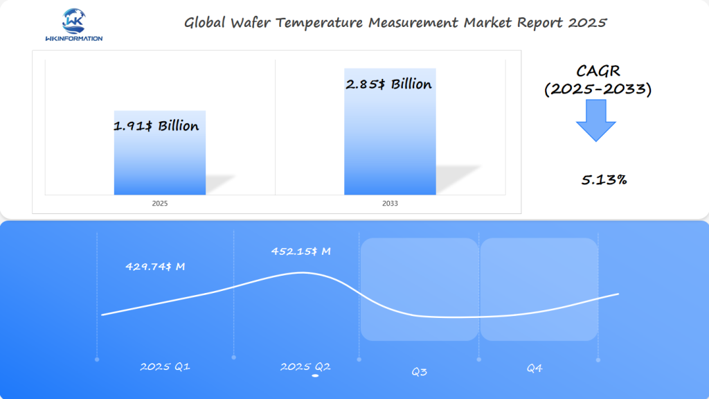
The wafer temperature measurement market is projected to grow from $1.91B in 2025 to $2.85B by 2033, driven by semiconductor demand and advanced technologies.
- Last Updated:
Projected Market Insights for Wafer Temperature Measurement in Q1 and Q2 of 2025
The Wafer Temperature Measurement market is set to reach $1.91 billion in 2025, with a CAGR of 5.13% from 2025 to 2033. In Q1, the market is expected to generate approximately $429.74 million, driven by the demand for precision temperature measurements in semiconductor manufacturing. By Q2, the market is expected to rise to $452.15 million as advancements in wafer-level packaging and growing semiconductor applications in various industries, including consumer electronics and automotive, continue to boost demand.
The U.S., Japan, and Germany are leading regions for this market. The U.S. maintains its position as a global leader in semiconductor innovation, while Japan and Germany remain strong players in the technology and industrial manufacturing sectors. As the push for smaller and more efficient electronic devices continues, the wafer temperature measurement market is anticipated to grow steadily.
Understanding the Upstream and Downstream Industry Chains for Wafer Temperature Measurement
To navigate the wafer temperature measurement market successfully, it’s essential to have a deep understanding of its complex industry chains.
The Upstream Supply Chain
The upstream supply chain is the backbone of this ecosystem. It includes all the necessary components and technologies that power wafer temperature measurement devices. Here are some key elements:
- Sensor elements such as thermocouples and infrared sensors
- Transmitters like RF/Wi-Fi/Bluetooth
- Power sources ranging from batteries to advanced wireless power transfer systems
These components are essential for achieving accurate and dependable temperature measurements in semiconductor manufacturing processes.
The Downstream Demand
Downstream demand refers to the specific areas where these advanced measurement solutions are utilized. In the semiconductor industry, accurate wafer temperature readings are crucial for maintaining product quality and enhancing production efficiency. Here are some key applications:
- Monitoring 300mm wafers, which dominate production activities due to their enhanced capacity for integrated circuits
- Optimizing processes such as annealing and chemical vapor deposition (CVD) by precisely controlling temperatures
In this ever-changing landscape, it’s vital for businesses looking to seize growth opportunities in the wafer temperature measurement market to understand both upstream supply chains and downstream applications. This knowledge enables companies to position themselves better amidst evolving technological demands in semiconductor manufacturing processes.
Key Trends Driving the Wafer Temperature Measurement Market Forward
The wafer temperature measurement market is evolving rapidly, with several key trends shaping its trajectory. Automation and IoT integration stand as major drivers in this landscape, ushering a new era of efficiency and precision. These technologies enable real-time data acquisition and remote monitoring, crucial for maintaining optimal conditions in semiconductor manufacturing processes.
1. Automation
The semiconductor industry is moving towards automated manufacturing processes, which greatly increases the need for accurate temperature monitoring. Automated systems require little human involvement, minimizing the chances of mistakes and improving repeatability and uniformity in production.
2. IoT Integration
The integration of Internet of Things (IoT) solutions facilitates seamless communication between devices. IoT-enabled temperature sensors can transmit data wirelessly to centralized control systems, ensuring timely responses to any deviations from desired temperature ranges. This connectivity not only boosts efficiency but also contributes to predictive maintenance strategies.
Adopting advanced measurement technologies is essential for meeting the industry’s growing demands. Innovations such as wireless sensors offer non-intrusive and highly accurate measurement capabilities. These devices are equipped with sensor elements like thermocouples or infrared sensors and leverage RF/Wi-Fi/Bluetooth for data transmission.
The evolution of wafer temperature measurement solutions aligns with the semiconductor sector’s overarching goal of optimizing production while minimizing contamination risks. As technology continues to advance, businesses must stay attuned to these trends to maintain competitive advantage and capitalize on emerging opportunities within this dynamic market space.
Challenges in Accurate Wafer Temperature Measurement for Semiconductor Manufacturing
Achieving precise measurement accuracy in wafer temperature monitoring within the semiconductor industry presents several operational challenges. These challenges stem from the high precision required to ensure that wafers meet stringent quality standards. Variations in temperature measurement can lead to significant defects, impacting both yield and performance of semiconductor devices.
Contamination risks further complicate the process. The presence of contaminants can skew readings, affecting measurement reliability. This directly influences the overall product quality, as impurities on the wafer surface can interfere with sensor readings and distort data.
Operational Challenges
- High precision requirements demand advanced calibration techniques.
- Environmental factors such as humidity and dust can alter sensor performance.
- Equipment malfunctions or misalignments during production processes may lead to erroneous data.
Contamination Risks
- Contaminants such as particles or residues can affect measurement accuracy.
- Regular maintenance and cleanroom environments are essential to minimize risks.
This highlights the need for advanced solutions that tackle these challenges, leading to innovation in sensor technology and process automation for improved reliability and efficiency.
Geopolitical Impact on the Wafer Temperature Measurement Market
Geopolitical factors are playing an increasingly crucial role in shaping the wafer temperature measurement market. The ongoing U.S.-China trade tensions have a notable impact, affecting both the supply chain and market dynamics. As these two powerhouses engage in trade negotiations and impose tariffs, companies within the semiconductor industry face operational challenges that can influence pricing, availability of components, and investment strategies.
Global trade dynamics further complicate the landscape. For companies operating across different regions, navigating the complexities of international regulations and trade agreements becomes essential. The ability to source materials and distribute products efficiently is often hindered by geopolitical uncertainties.
Key Geopolitical Influences
U.S.-China Trade Relations
The contentious U.S.-China trade relationship significantly affects how businesses strategize their production and distribution processes. Companies might need to diversify their supply chains or seek alternative markets to mitigate risks associated with tariffs or import restrictions.
Supply Chain and Market Access
The ripple effects of global trade policies, such as those stemming from the U.S.-China trade war, can create bottlenecks or open new opportunities for businesses. Understanding these supply chain impacts is crucial, as it depends on regional alliances and economic agreements.
Understanding these geopolitical influences is vital for companies aiming to remain competitive. Anticipating shifts in global trade policies can provide a strategic advantage in maintaining a resilient supply chain and accessing new market opportunities.
Market Segmentation: Types and Applications of Wafer Temperature Measurement Technologies
Understanding the various market segments in the wafer temperature measurement industry helps us understand the different devices available, each designed for specific needs in semiconductor manufacturing. Among these devices, wireless sensors have become popular because they can measure without being intrusive and can monitor in real-time. These sensors often use advanced technologies like thermocouples or infrared sensors along with transmitters such as RF, Wi-Fi, or Bluetooth to ensure high accuracy and flexibility.
Types of Wafer Temperature Measurement Devices
1. Wireless Sensors
- Features: Non-intrusive measurement, high precision, flexibility in installation.
- Benefits: Real-time data transmission, reduced risk of contamination, easy integration into existing systems.
2. Infrared Sensors
- Features: Contactless temperature measurement, rapid response time.
- Benefits: Ideal for measuring moving wafers, enhanced safety by preventing direct contact.
3. Thermocouples
- Features: Direct contact measurement, robust construction.
- Benefits: Cost-effective for high-volume applications, adaptable to various environments.
Key Application Areas
Wafer temperature measurement technologies are crucial in several areas of the semiconductor industry:
- 300mm Wafers: These larger wafers make up a significant portion of production activities. Accurate temperature control during processing is vital to ensure product quality and operational efficiency.
- Process Optimization: Advanced measurement technologies contribute to streamlined manufacturing processes by providing precise data that aids in reducing cycle times and enhancing yield rates.
- Contamination Control: By offering reliable and non-contact measurements, these technologies play a crucial role in minimizing contamination risks inherent in semiconductor manufacturing environments.
The wide range of devices and their applications highlights the importance of selecting the right technology for specific manufacturing needs. This careful choice ensures optimal performance and supports advancements in the rapidly evolving semiconductor sector.
Wafer Temperature Measurement in Semiconductor and Electronics Manufacturing
Wafer temperature measurement is crucial in semiconductor and electronics manufacturing. It ensures precise temperature control, which is essential for maintaining product quality and operational efficiency.
Importance of Accurate Thermal Conditions
In various manufacturing processes such as:
- Wafer bonding
- Etching
- Deposition
- Doping
Maintaining accurate thermal conditions is key to achieving the desired material properties and device performance.
Role of High-Precision Temperature Sensors
To monitor wafer temperatures during fabrication, high-precision temperature sensors are commonly used. These include:
- Thermocouples
- Infrared sensors
- Pyrometers
Benefits of Effective Temperature Management
Accurate temperature management brings several benefits, including:
- Preventing defects
- Enhancing yield
- Reducing the risk of thermal-related failures in complex electronic devices
Growing Demand for Advanced Measurement Technologies
As manufacturing processes become more advanced and miniaturized, the demand for even more accurate and reliable wafer temperature measurement technologies continues to grow. This trend drives innovations in sensor technology and data analytics.
Global Insights into the Wafer Temperature Measurement Market
The wafer temperature measurement market is experiencing substantial growth, with major contributions from key regions such as the U.S., Japan, and Germany. These countries are instrumental in driving growth in this industry due to their advanced semiconductor manufacturing capabilities and technological expertise.
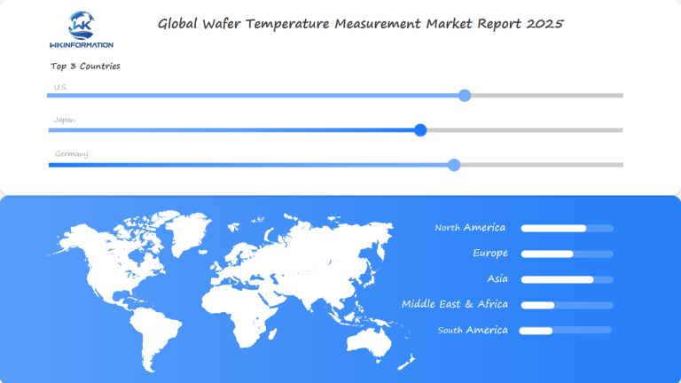
U.S. Market Demand for Advanced Wafer Temperature Measurement Solutions
- The U.S. has a strong semiconductor industry that invests heavily in research and development. As a global leader in technology innovation, the country needs precise wafer temperature measurement solutions to improve production efficiency and maintain competitive advantages.
- This need is evident from the U.S.’s substantial exposure to the Taiwanese semiconductor industry, which highlights the country’s reliance on accurate temperature measurement solutions.
- There are opportunities to develop advanced temperature measurement devices that cater to emerging technologies such as IoT and AI-driven manufacturing processes.
Japan’s Technological Leadership in Wafer Temperature Measurement
Japan, renowned for its advanced electronics industry, plays a major role in the worldwide wafer temperature measurement market. The country’s dedication to maintaining top-notch production quality demands the use of sophisticated measurement techniques for consistent product performance.
- Businesses can consider collaborating with Japanese companies to incorporate innovative sensor technologies into their current systems, thus broadening their market presence.
Germany’s Influence on Wafer Temperature Measurement Standards and Innovations
Germany is Europe’s center for technological advancements, with a focus on precision engineering and manufacturing excellence. The country’s semiconductor industry relies on accurate temperature monitoring to optimize process control and reduce waste.
There is potential for growth by leveraging Germany’s expertise in automation and Industry 4.0 initiatives, offering opportunities for innovative solutions that align with sustainable manufacturing practices.
These regional insights highlight the various opportunities available within the global market. By leveraging each region’s unique strengths, companies can drive innovation and meet the changing demands of the semiconductor industry. Additionally, exploring the porous ceramic vacuum chuck market for semiconductor wafers could also present new avenues for growth and development in this sector.
The Future of Wafer Temperature Measurement: Advancements, Opportunities, and Conclusion
The Wafer Temperature Measurement Market is on the verge of significant technological advancements. Emerging innovations in sensor technology and wireless communication are expected to further improve measurement accuracy and efficiency. Key developments include:
- Integration of AI and Machine Learning: These technologies promise to enhance predictive analytics for temperature trends, helping manufacturers optimize processes.
- Advanced Wireless Solutions: Increased use of wireless power transfer systems and robust connectivity options, such as IoT-enabled devices, will drive operational flexibility.
- Miniaturization of Sensor Components: Reducing the size of sensor elements while maintaining performance can open new application possibilities.
The market’s growth potential is vast, with emerging opportunities particularly evident in regions like the U.S., Japan, and Germany. Businesses should leverage these advancements to stay competitive.
For industry professionals and stakeholders eager to keep up with these developments, Wkinformation Research offers comprehensive reports. Engage with these resources to gain insights into the latest trends and future directions of the wafer temperature measurement landscape.
Stay informed and strategically positioned in this dynamic sector by accessing ongoing research updates from reliable sources like Wkinformation Research.
Competitive Landscape in the Wafer Temperature Measurement Market
The wafer temperature measurement market is shaped by several key players, each striving to innovate and capture a larger share of this burgeoning industry.
- KLA Corporation — USA
- Phase IV Engineering Inc. — USA
- Thermo Electric Co. — USA
- SPM Instrument AB — Sweden
- ERS electronic GmbH — Germany
Overall
| Report Metric | Details |
|---|---|
| Report Name | Global Wafer Temperature Measurement Market Report |
| Base Year | 2024 |
| Segment by Type |
|
| Segment by Application |
|
| Geographies Covered |
|
| Forecast units | USD million in value |
| Report coverage | Revenue and volume forecast, company share, competitive landscape, growth factors and trends |
The wafer temperature measurement market shows strong growth potential due to the increasing complexity of semiconductor manufacturing and the rising demand for high-performance chips. Advanced packaging technologies also contribute to a positive market outlook, ensuring ongoing demand. The forecast predicts continued growth, supported by trends such as IoT integration, automation, and non-contact measurement technologies.
Technological advancements like high-resolution systems and energy-efficient designs are transforming the industry. Emerging markets in Asia-Pacific and Latin America present significant opportunities, backed by investments in infrastructure and manufacturing. As the market develops, its emphasis on sustainability and precision will reinforce its role in semiconductor innovation.
Global Wafer Temperature Measurement Market Report (Can Read by Free sample) – Table of Contents
Chapter 1: Wafer Temperature Measurement Market Analysis Overview
- Competitive Forces Analysis (Porter’s Five Forces)
- Strategic Growth Assessment (Ansoff Matrix)
- Industry Value Chain Insights
- Regional Trends and Key Market Drivers
- Wafer Temperature Measurement MarketSegmentation Overview
Chapter 2: Competitive Landscape
- Global Wafer Temperature Measurementplayers and Regional Insights
- Key Players and Market Share Analysis
- Sales Trends of Leading Companies
- Year-on-Year Performance Insights
- Competitive Strategies and Market Positioning
- Key Differentiators and Strategic Moves
Chapter 3: Wafer Temperature Measurement Market Segmentation Analysis
- Key Data and Visual Insights
- Trends, Growth Rates, and Drivers
- Segment Dynamics and Insights
- Detailed Market Analysis by Segment
Chapter 4: Regional Market Performance
- Consumer Trends by Region
- Historical Data and Growth Forecasts
- Regional Growth Factors
- Economic, Demographic, and Technological Impacts
- Challenges and Opportunities in Key Regions
- Regional Trends and Market Shifts
- Key Cities and High-Demand Areas
Chapter 5: Wafer Temperature Measurement Emerging and Untapped Markets
- Growth Potential in Secondary Regions
- Trends, Challenges, and Opportunities
Chapter 6: Product and Application Segmentation
- Product Types and Innovation Trends
- Application-Based Market Insights
Chapter 7: Wafer Temperature Measurement Consumer Insights
- Demographics and Buying Behaviors
- Target Audience Profiles
Chapter 8: Key Findings and Recommendations
- Summary ofWafer Temperature Measurement Market Insights
- Actionable Recommendations for Stakeholders
Access the study in MULTIPLEFORMATS
Didn’t find what you’re looking for?
TALK TO OUR ANALYST TEAM
Need something within your budget?
NO WORRIES! WE GOT YOU COVERED!
Call us on: +1-866-739-3133
Email: infor@wkinformation.com
Why is wafer temperature measurement important in the semiconductor industry?
Wafer temperature measurement is crucial in the semiconductor industry as it ensures accurate processing during manufacturing, impacting product quality and performance. It plays a vital role in maintaining optimal conditions for various semiconductor fabrication processes.
What are the projected growth and market value of the wafer temperature measurement market by 2025?
The wafer temperature measurement market is expected to grow significantly, with estimates indicating a substantial increase in market value by 2025. This growth is driven by advancements in technology and increasing demand for precision in semiconductor manufacturing.
What are the key trends driving the growth of the wafer temperature measurement market?
The wafer temperature measurement market is being influenced by several key trends:
- Increased automation within manufacturing processes
- Integration of IoT technologies
These advancements enable enhanced measurement accuracy and efficiency, meeting the evolving demands of the semiconductor industry.
What challenges are faced in achieving accurate wafer temperature measurements during semiconductor manufacturing?
Achieving accurate wafer temperature measurements in semiconductor manufacturing comes with its own set of challenges:
- Risks of contamination: Any foreign particles or substances on the wafer can interfere with the temperature measurement, leading to unreliable results.
- Operational challenges: Maintaining precise conditions during manufacturing processes is crucial. Any fluctuations in temperature, pressure, or other environmental factors can impact the accuracy of the measurements.
How do geopolitical factors influence the wafer temperature measurement market?
Geopolitical factors, especially U.S.-China trade relations, have a significant impact on the wafer temperature measurement market. Global trade dynamics can affect supply chains and market access for companies operating in various regions, thereby influencing overall market stability.
What types of wafer temperature measurement technologies are available in the market?
The market offers different kinds of devices for measuring wafer temperature. These include wireless sensors that have advantages like flexibility and easy integration. These technologies are used in important areas, especially for 300mm wafers.
RECENT REPORTS
Our clients